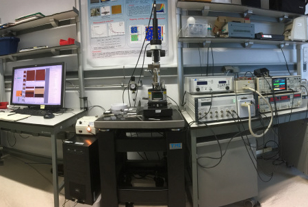
nano-Dielectric Spectroscopy set-up
|
The overwhelming interest in
nanostructured materials during the last years has highlighted the lack of
spatial resolution in BDS measurements. As a result, an experimental method
that combines the BDS advantages with the outstanding spatial resolution
of the Atomic Force Microscope (AFM) has been developed by combining standard
AFM equipments in with a dedicated lock-in amplifier.
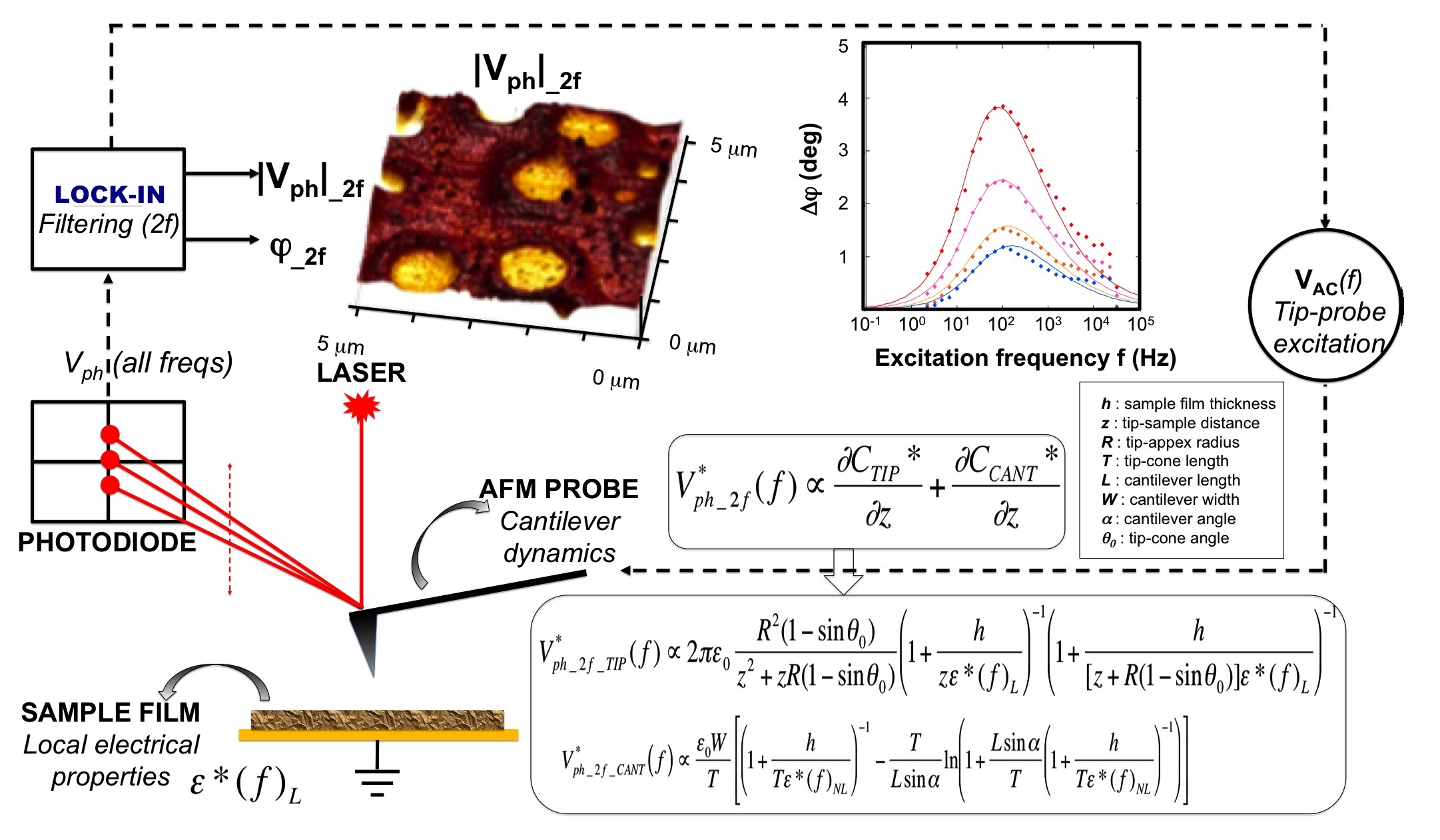
In this approach (see Figure below), a sinusoidal voltage Vac(f) is applied to the AFM conductive probe, while maintained a few nanometers above the sample, and the harmonic components of the photodiode signal at 2f (the oscillation amplitude, |VPh|, and the phase) are measured. The characteristics of this signal are originated in the electrical properties of the sample film, including dissipative effects. This set-up allows to determine the local dielectric relaxation behavior of thin films, with up to 20 nm lateral resolution, in a frequency range from 1 to 1MHz. |
INSTRUMENT CHARACTERISTICS |
Atomic Force Microscope: MultiMode Bruker
Low-noise Lock-in amplifier: SRS865A SRS
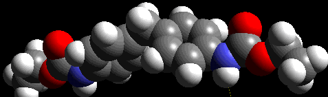
Samples: Thin films on conductive support |
|
|

|
Contact
|Where
we are | Last updated December 2017